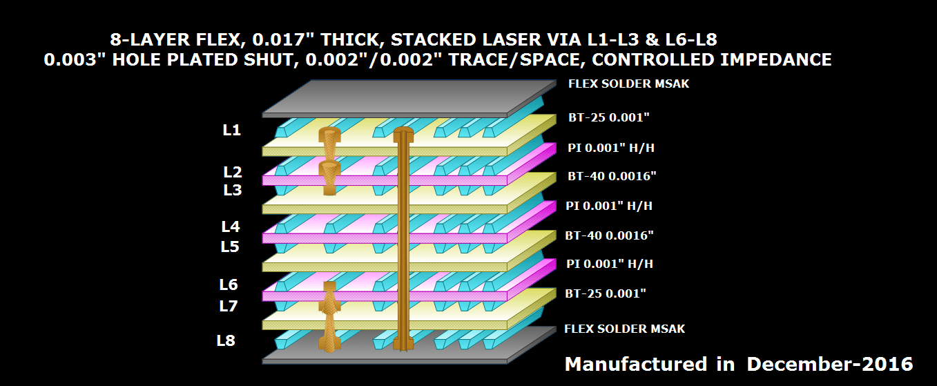
PCB stack-up of 8-layer test board
$ 10.00 · 4.9 (489) · In stock

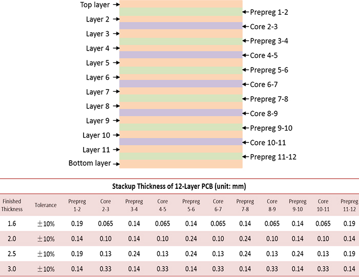
PCB Layer Stackup, PCB Stackup Design

Targets are modeled as entering at locations p1, p2, …, p4 at the

α Vs ρ, single-source Pareto traffic

Selecting a PCB stack-up for EMC compliance – TechnieX

Deciding the Right Build-Up for A Multi-Layer PCB Design - PCB Power

PDF) Pre-layout multi-layer PDN model for high-speed board
Understanding PCB Stackup: Materials and Layer Configuration - Rush PCB

4 Layer PCB Layout Tutorial, Stack-up design, and Cost of manufacturing - Absolute Electronics Services

A schematic diagram of sodium aerosol sampling system installed in

Mean queue length E[n] as a function of the normalized load ρ, (AR